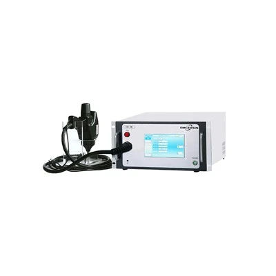
Most ESD protection failures do not trace back to a wrong component choice - they trace back to a current path that was never designed.
1. Start with the Closed Loop: Four Levers in ESD Test and Protection
ESD protection has a single objective: confine the current path so that the chip and the interface keep working. On the test side the sequence is linear: charge generation → contact or air discharge → disturbance of the equipment under test (EUT) → verdict against performance criteria A/B/C. The human body model (HBM) describes exactly the instant when a charged person touches the equipment - discharge current flows through the enclosure and the connectors into the product. On the protection side there are four levers: port suppression, discharge path, isolation and grounding, and system-level verification. They are not parallel options but successive fallbacks - the port absorbs the first wave, the discharge path carries the bulk current away, isolation and grounding cut the coupling, and system-level verification proves that the whole chain actually works.

Fig. 1 | ESD test and protection loop
2. HBM, CDM and MM: Three Models, Three Waveforms, Three Failure Mechanisms
Pick the wrong model and every subsequent test is wasted.
HBM (human body model): simulates a charged person touching the equipment. It is the most widely used model, tested at 2 kV, 4 kV and 8 kV, with the waveform set by a 150 pF / 330 Ω discharge network.
CDM (charged device model): simulates a device that has charged up on the production line and then discharges rapidly. Its current rises fastest - in the sub-nanosecond range - and the larger the package, the higher the risk.
MM (machine model): simulates discharge from conductive tools and robot arms. Its energy profile differs from HBM and targets process steps more directly.
A single chip may face all three models, yet the three do not fail in the same place: HBM strikes the interface, CDM strikes the internal bond pads. Equipment makers care about HBM; chip makers must pass all three.
|
Model |
Discharge scenario |
Key parameters |
Primary owner |
|
HBM - human body model |
A charged person touching the equipment |
150 pF + 330 Ω; 2 / 4 / 8 kV |
Equipment makers |
|
CDM - charged device model |
A device charged on the line, then rapidly discharged |
Sub-nanosecond current rise; larger packages are riskier |
Chip makers |
|
MM - machine model |
Conductive tools and robot arms |
Energy profile different from HBM |
Process engineering |
Table 1 | Three ESD discharge models
3. Test Levels: Contact and Air Discharge Are Two Separate Numbers
Levels are not chosen by intuition; they follow product category, port type and the intended operating environment. The four common levels are:
|
Level |
Contact discharge |
Air discharge |
Typical application |
|
Level 1 |
±2 kV |
±4 kV |
General consumer equipment |
|
Level 2 |
±4 kV |
±8 kV |
Commercial and industrial equipment |
|
Level 3 |
±6 kV |
±15 kV |
Heavy industry environments |
|
Level 4 |
±8 kV |
±15 kV |
Harsh industrial sites |
Table 2 | ESD test levels
4. System-Level Setup: HCP, VCP and AE Are All Mandatory
Indirect discharge on tabletop equipment runs entirely through the coupling planes; get the setup wrong and even a precisely applied level means nothing.
The standard setup comprises the ESD gun (ES), the equipment under test (EUT), the horizontal coupling plane (HCP), the vertical coupling plane (VCP), auxiliary equipment (AE) and a functional monitor. The EUT sits on the HCP at the standard distance (tabletop equipment is separated by a 0.1 m insulating support), and the gun discharges to the edges of the HCP and VCP, which tests the EUT's immunity to indirect disturbance.
Two discharge methods must be kept apart:
Contact discharge: the tip electrode touches a metal part of the EUT or the coupling plane first, then the discharge is triggered - good repeatability, so this method is preferred.
Air discharge: the rounded electrode approaches a non-conductive surface (plastic enclosure, key gaps) until breakdown occurs - closer to real-world use, but far more scattered.

Fig. 2 | System-level test setup
5. How ESD Current Enters the Equipment: Four Paths, Each Worse Than the Last
Protection design rests on one first principle: a low-impedance discharge path matters more than filtering added afterwards.
When the gun fires, current is injected at the front-panel metal, connector shells, key surfaces, PCB ground and cable shields, and can reach the chip ports inside. From there it takes one of four paths:
Path A - enclosure discharge. Current returns to earth through the low-impedance enclosure. This is the ideal path, and steering current here is the whole design goal.
Path B - cable coupling. Current couples onto cables and runs into the attached auxiliary equipment, causing collateral failure.
Path C - PCB conduction. Current spreads along the ground plane, and ground bounce upsets nearby sensitive circuits.
Path D - straight into the chip. Every layer of protection has failed, energy is dumped into the chip port, and the result is usually a hard failure.
The entire design effort is to force current out of path D and back into path A.

Fig. 3 | Four paths for ESD current
6. Six Failure Modes: Separate Hard Failures from Soft Failures
A hard failure is fixed by replacing a part; a soft failure comes back as a batch rework. Telling them apart is the precondition for choosing the right protection strategy.
Hard failures (physical damage, not recoverable):
Dielectric breakdown: gate oxide or dielectric layers are damaged and the chip is punched through on the spot.
Metal burnout: interconnects or solder joints melt, typically on high-current paths.
Latch-up: the parasitic thyristor is triggered into conduction, the supply shorts to ground, and a power cycle will not save it.
Interface damage: I/O ports and transceivers fail - the usual cause of a peripheral that "mysteriously disappears."
Soft failures (no physical damage, recoverable but fatal in the field):
Reset and hang: logic states are disturbed and the unit looks normal after a restart.
Parameter drift: leakage current or thresholds shift quietly, leaving a defect that surfaces after volume production.
A soft failure "comes back to life" once it leaves the lab, and in the field it turns into batch complaints - the type equipment makers fear most.
|
Type |
Failure mode |
Manifestation |
|
Hard |
Dielectric breakdown |
Gate oxide or dielectric damaged; chip punched through |
|
Hard |
Metal burnout |
Interconnects or solder joints melt |
|
Hard |
Latch-up |
Parasitic thyristor conducts; supply shorts to ground |
|
Hard |
Interface damage |
I/O ports and transceivers fail |
|
Soft |
Reset / hang |
Logic states disturbed; looks normal after restart |
|
Soft |
Parameter drift |
Leakage current or thresholds shift slowly |
Table 3 | Six ESD failure modes
7. Three Stages of Protection: Divert, Clamp, Isolate
No single device survives 8 kV on its own; staged protection is the mainstream approach.
Gas discharge tube (GDT): coarse protection with the highest current-handling capability, but slow response and high residual voltage. It sits at the outermost layer and takes the first hit.
TVS diode: fast response and low clamping voltage. It sits on the inner layer for fine protection and holds the residual voltage down to a level the chip can tolerate.
Isolation and filtering (common-mode chokes, ferrite beads, isolators): block the coupling path and suppress residual disturbance.
The classic combination is a three-stage GDT + current-limiting resistor + TVS chain: divert first (the GDT carries most of the energy away) → clamp next (the TVS holds the voltage down) → then protect the internal circuit (the resistor limits the current reaching the chip). The order cannot be swapped - put a TVS alone at the front and the first large surge will destroy it.
|
Stage |
Device |
Function |
Position |
|
First stage |
Gas discharge tube (GDT) |
Diverts the bulk current; slow response, high residual voltage |
Outermost layer |
|
- |
Current-limiting resistor |
Limits the current reaching the chip |
Between GDT and TVS |
|
Second stage |
TVS diode |
Fast clamping, low residual voltage |
Close to the protected circuit |
|
Auxiliary |
Isolation and filtering |
Blocks coupling, suppresses residual disturbance |
Between port and chip |
Table 4 | Protection devices and staged protection
8. Five PCB Layout Rules: A Misplaced Device Is a Missing Device
The further a device sits from the interface, the more protection it loses.
Put protection at the entry: the ESD device must sit against the connector, ahead of any branch.
Keep the discharge path short and straight: the trace from the interface to ground should be as short as possible; inductance in a long trace lifts the residual voltage.
Use many ground vias, placed close by: put a via next to each protection device to cut the inductance of the return path.
Keep sensitive circuits away from the entry: main chips, clocks and reset lines belong far from the connector and must not run parallel to the discharge path.
Route critical signals differentially: high-speed signals go differential and away from the board edge to reduce coupling pickup.
The right-versus-wrong comparison is blunt: with the device far from the interface, the discharge loop area grows, induced voltage rises, and the protection is decorative. With the device against the interface, current is escorted out at the door and the internal circuit never sees the surge.

Fig. 4 | PCB protection layout
9. Pre-Delivery Checklist: Four Blocks, Item by Item
ESD design is not a single-component problem; it is a problem of paths, partitioning and system verification. In design review, tick off four blocks:
Port protection: ESD devices at every interface, short discharge paths, shield shell and shield layer reliably bonded.
PCB design: protection devices at the entry, sufficient ground vias, sensitive traces away from the entry.
System design: low enclosure discharge impedance, continuous cable shielding, clear partitioning of interface circuits.
Verification: test at the specified levels (both polarities, repeated discharges), monitor functions and parameters, record every failure.
Recording failure symptoms is the step most often skipped, yet it is the entire input to the next design revision. A failure without a record is a failure wasted.
|
Block |
Check item 1 |
Check item 2 |
Check item 3 |
|
Port protection |
ESD devices at every interface |
Short discharge paths |
Shield shell and shield layer reliably bonded |
|
PCB design |
Protection devices at the entry |
Sufficient ground vias |
Sensitive traces away from the entry |
|
System design |
Low enclosure discharge impedance |
Continuous cable shielding |
Clear partitioning of interface circuits |
|
Verification |
Both polarities, repeated discharges |
Monitor functions and parameters |
Record every failure |
Table 5 | ESD design checklist
In one sentence: forcing ESD current out of "straight into the chip" and back into "enclosure discharge" does not depend on a miracle component - it depends on a six-step closed loop: the right model, the right level, a designed path, staged protection, tight layout, and verification with records.